
N-type and P-type Semiconductors
In intrinsic semiconductors the number of holes is equal to the number of free electrons. The thermal agitation continuously produce new electron hole pairs , whereas other hole electron pairs disappear due to the process of recombination.
where n= no of electrons
p= no of holes
Ni= intrinsic concentration
Before going to the concept mass action law, we need to know about donors and acceptor impurities which are used to make extrinsic semiconductors.
DONOR impurity: If the dopant has 5 valence electrons that impurity is called as donor impurity.
(Ex: Arsenic, Antimony, Phosphorus-Pentavalent atoms)
 |
| n-type semiconductor |
N-type semiconductor:
In the above picture shows the crystal structure of pentavalent atom with silicon atoms. The impurity atoms will displace some of the silicon atoms in the crystal lattice. Four of the five valence electrons will occupy covalent bonds, and the fifth will be nominally unbound and will be available as a carrier of current . The energy required to detach this fifth electron from the atom is of the order of only 0.01ev for Ge and 0.05ev for Si. Suitable pentavalent impurities should be picked for getting n-type semiconductor.
The impurities which can donate the electron carriers are called as DONOR IMPURITIES. When donor impurities added to the pure semiconductor , allowable energy levels are introduced a very small distance below the conduction band. These new allowable levels are essentially a discrete level. Because the added impurity atoms far apart in the crystal structure, and their interaction is small.
ACCEPTOR impurity:
If the dopant has 3 valence electrons that type of impurity is called as acceptor impurity.
(Ex: boron, gallium, indium- trivalent atoms)
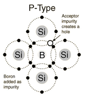 |
| P-type semiconductor |
P-type semiconductor:
In the above picture shows a trivalent impurity i.e Boron added to Silicon atoms then three of the covalent bonds can be filled and the vacancy that exists in the fourth bond constitutes a hole. Such impurities make available positive carriers because they create holes which can accept electrons. These impurities are also known as p-type impurities.
The amount of impurity which must be added to have an appreciable effect on the conductivity is very small . For example, if a donor impurity is added to the extent of 1 part in 10^8 , the conductivity of Ge (germanium) at 30℃ is multiplied by a factor of 12. When acceptor impurity is added to the semiconductor , they produce an allowable discrete energy level which is just above the valence band. Since very small amount of energy is required for an electron to leave the valence band and occupy the acceptor energy level, it follows that the holes generated in the valence band by these electrons constitute the largest number of carriers in the semiconductor material.
Energy band diagram for N-type and P-type semiconductors:
| Energy band diagram |
Ec- conduction band
Ef- fermi level
Ev- valance band
Eg- energy gap
Ef= Ed= donor energy level in case of n-type semiconductor
Ef= Ea= acceptor energy level in case of p-type semiconductor
Ef- fermi level
Ev- valance band
Eg- energy gap
Ef= Ed= donor energy level in case of n-type semiconductor
Ef= Ea= acceptor energy level in case of p-type semiconductor
Mass Action Law:
When you are adding an n-type of impurity it will decreases the number of holes, as well when we add a p-type impurity it will decreases the no of free electrons in a semiconductor. So , under thermal equilibrium condition , the product of free negative and positive concentrations is a constant independent of the amount of donor and acceptor impurity doping. This relationship is called the MASS ACTION LAW and is given by,
np=Ni^2
where n represents no of free electrons,
and p represents no of holes,
and Ni= intrinsic concentration as a function of temperature.
Charge Densities in a Semiconductor:
The mass action law gives the relation between the electron n and the hole p concentrations. These densities are further interrelated by the law of electrical neutrality , it will be explained as follows in algebraic form.
Let Nd= concentration of donor atoms
Na= concentration of acceptor atoms
Since a semiconductor is electrically neutral, the positive charge density must be equal to negative charge density.
Nd+p=Na+n
Consider an n-type material having Na=0;
n=Nd (n>>p)
Now consider a p-type material having Nd=0;
p=Na (p>>n)
Then from mass action law we concluded as,
np=Ni^2
if it is n-type semiconductor;
p=Ni^2/Nd
(where Nd= free electron concentration in n-type material)
p=Ni^2/Nd
(where Nd= free electron concentration in n-type material)
if it is p-type semiconductor :
n= Ni^2/Na
(where Na= hole concentration in p-type material).
n= Ni^2/Na
(where Na= hole concentration in p-type material).


No comments